PCB Cloning & Reverse Engineering Services
PCB cloning and reverse engineering is the process of reconstructing the design, layout, and functionality of an existing printed circuit board when original design files, schematics, or documentation are unavailable. At QUADRIONIX, reverse engineering is handled as a structured engineering process, combining physical analysis, component identification, and design reconstruction to enable reliable reproduction or redesign of legacy electronics. We support global organizations requiring accurate PCB cloning and reverse engineering services, particularly for legacy systems, discontinued products, and undocumented designs.
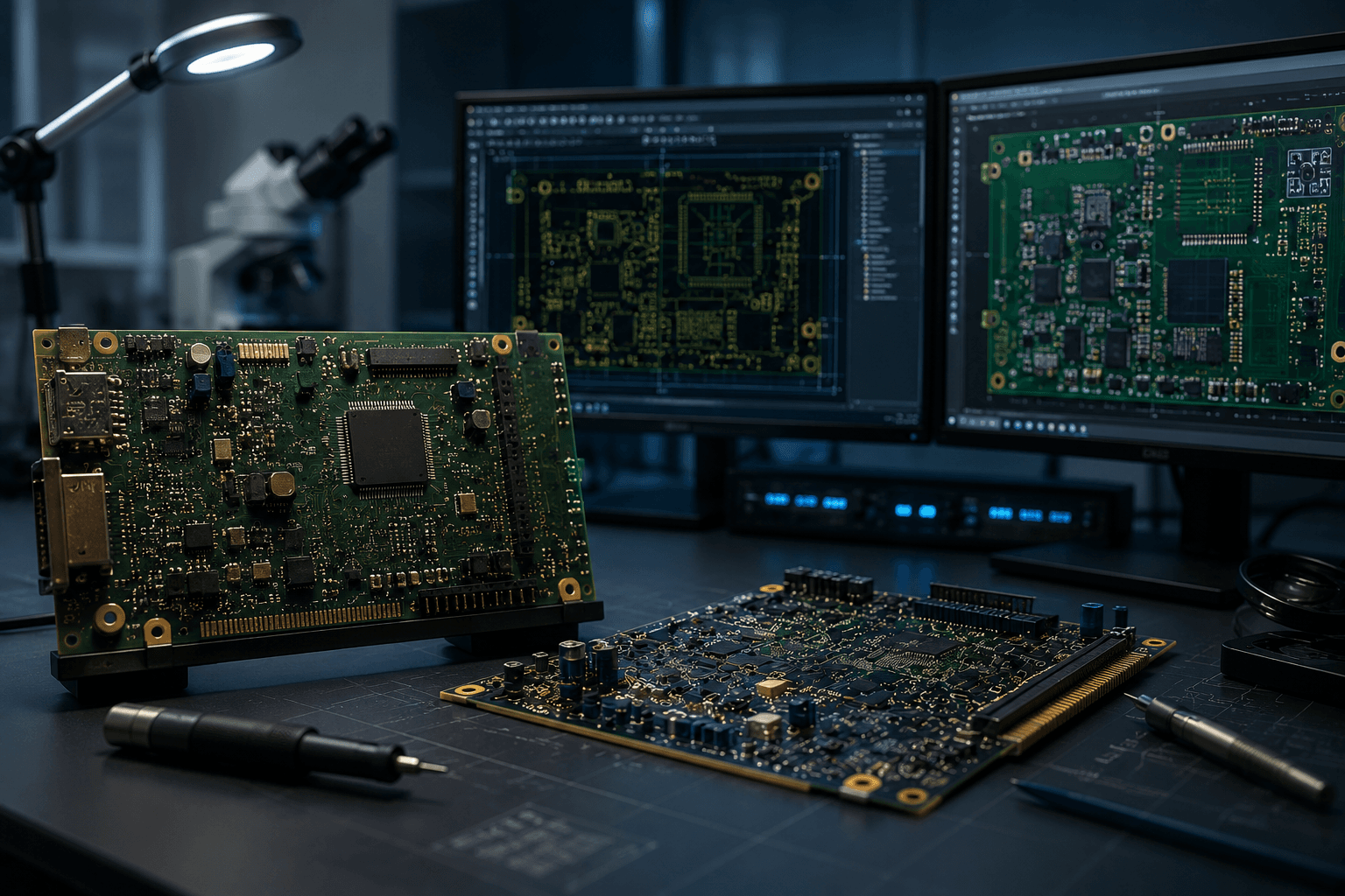
Service Overview
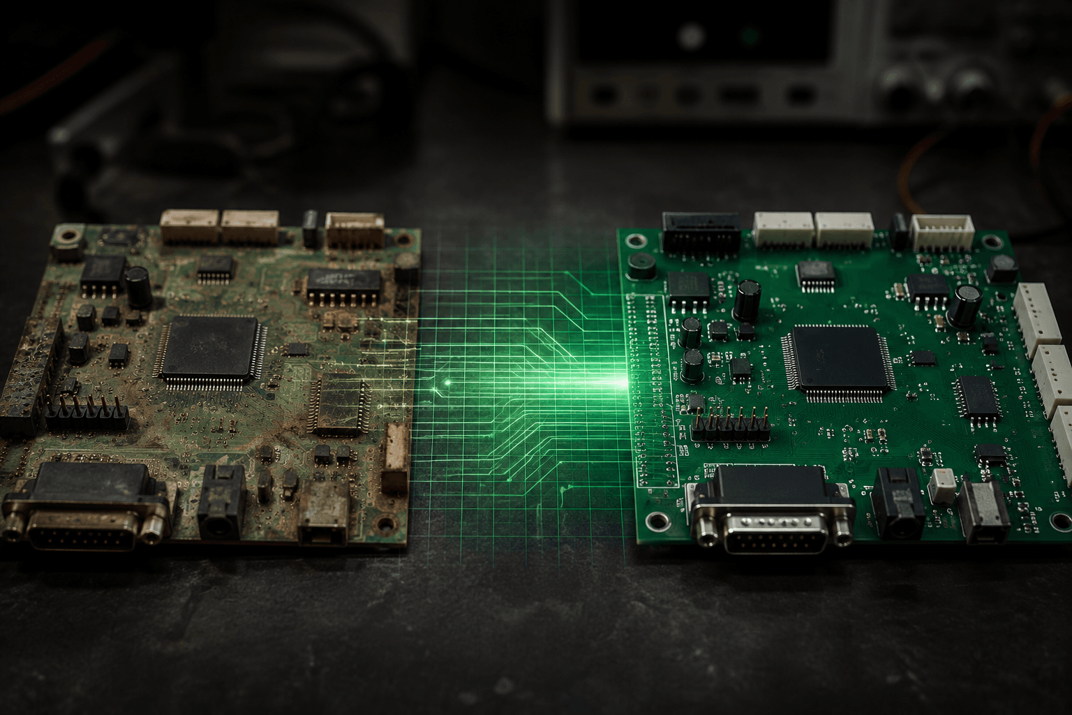
Many critical systems rely on electronics that are no longer supported, documented, or available in the market.
PCB cloning and reverse engineering services are designed to
- Recover design information
- Enable reproduction of existing boards
- Support maintenance and continuity of operations
This is particularly valuable where
- Original design files are lost
- Components are obsolete
- Suppliers are no longer available
Technical Specifications
Physical Board Analysis
Physical Board Analysis
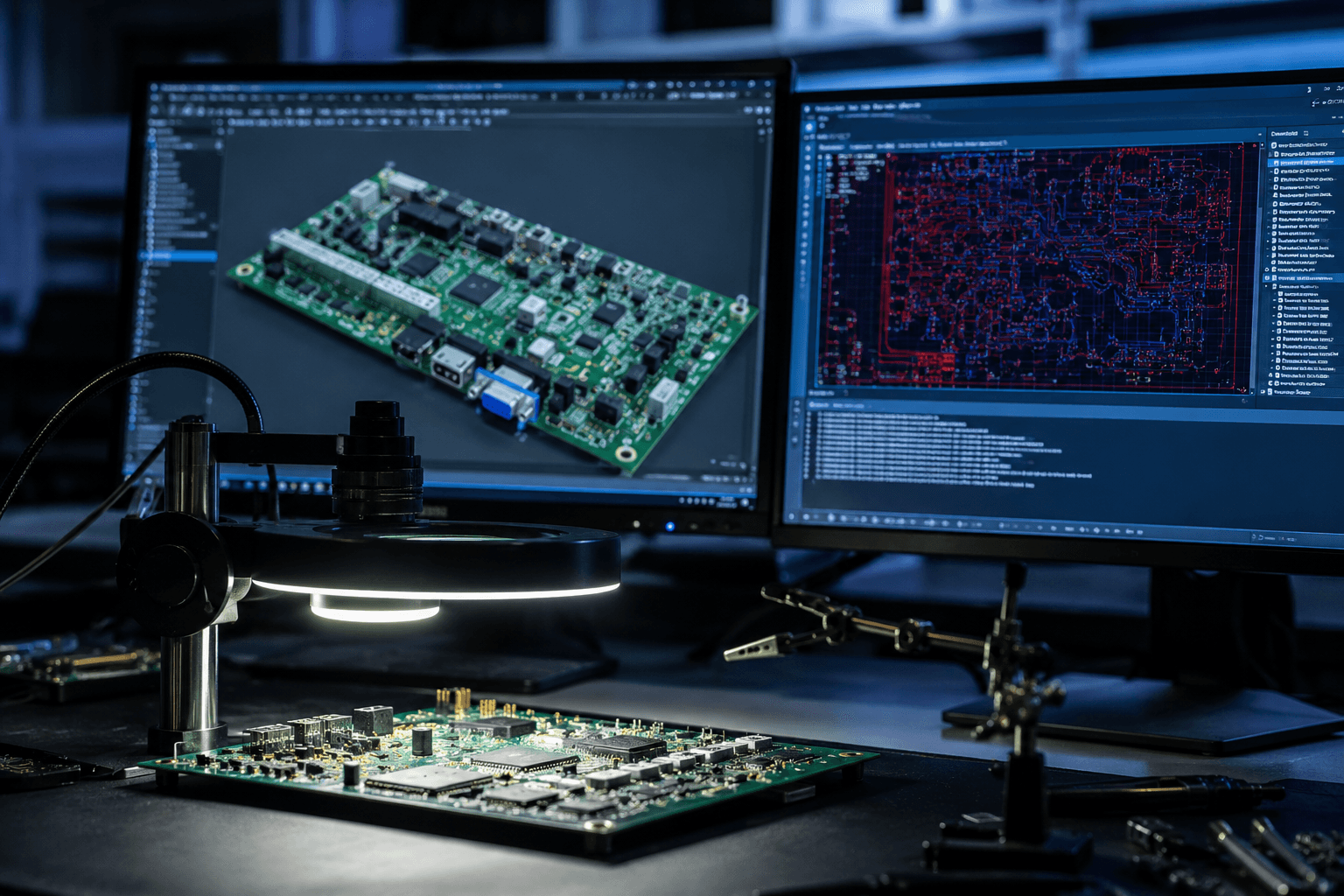
Visual inspection of PCB structure, layer identification (for multilayer boards), component mapping and identification.
Circuit Reconstruction
Schematic recreation, signal path tracing, functional block identification.
PCB Layout Reconstruction
Recreation of board layout, layer-by-layer reconstruction, alignment with manufacturable design standards.
Component Identification
Identification of active and passive components, lifecycle evaluation, replacement or alternate suggestions where required.
Design Output Preparation
Gerber files for fabrication, BOM reconstruction, documentation for assembly.
Pre-production verification
Every project is reviewed before production so design intent, manufacturability, and yield risks are understood early.
Functional Integrity
Preserving original circuit behavior, ensuring electrical equivalence, identifying critical design elements.
Manufacturability Alignment
Updating design for modern fabrication standards (if required), ensuring compatibility with current assembly processes.
Component Risk Handling
Identifying obsolete components, recommending viable alternatives, aligning replacements with performance requirements.
Design Improvement (Where Applicable)
Correcting known design limitations, improving manufacturability, enhancing reliability. This ensures that the recreated design is not only a copy — but usable and sustainable.
INSPECTION VERIFICATION PROTOCOL
Quality & Inspection
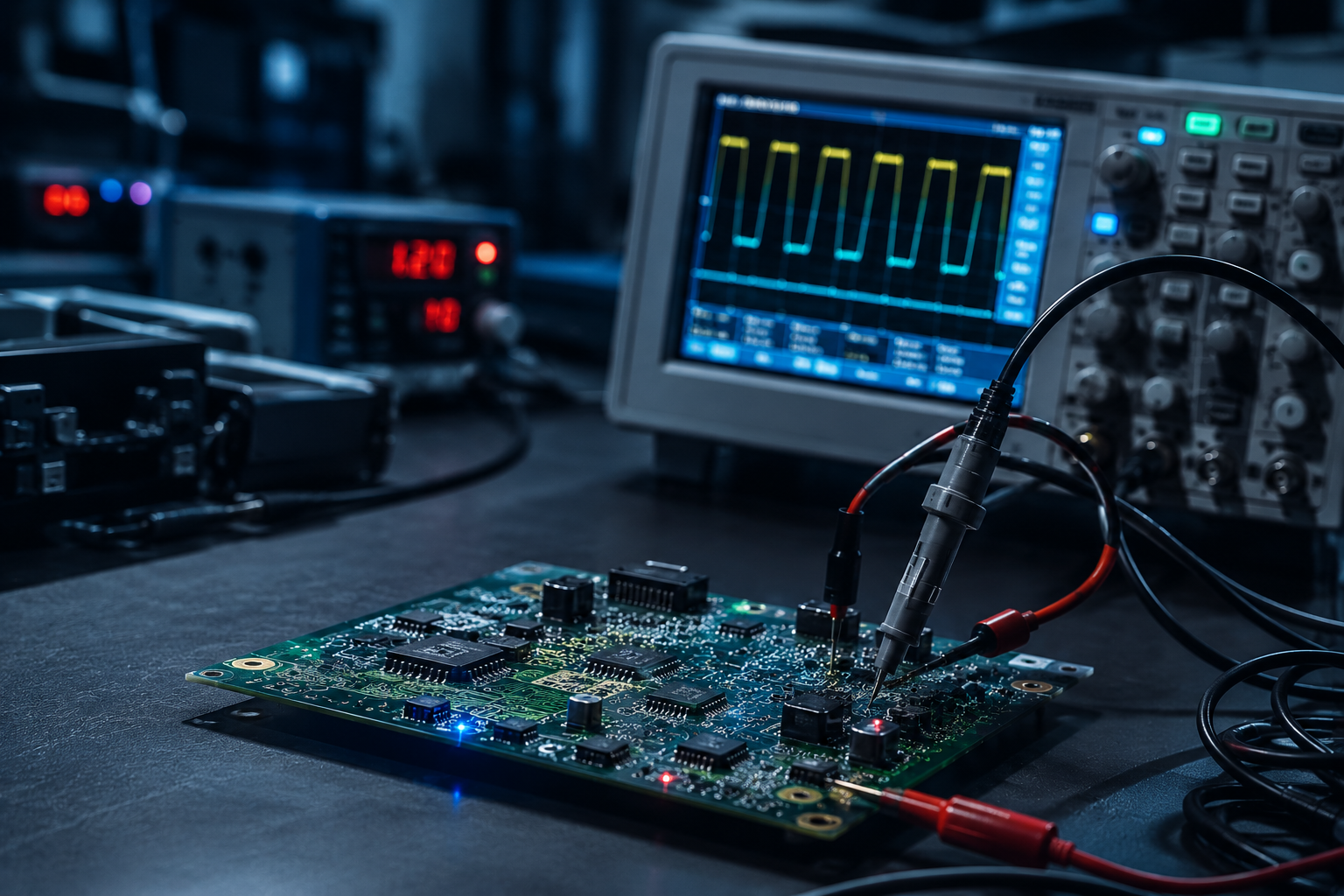
Fabrication quality is aligned with engineering intent through controlled inspection, process monitoring, and trace parameters auditing.
Applications
Where our execution makes a difference
industrial equipment maintenance
Precision engineered build configured for standard field deployment.
legacy electronics without documentation
Precision engineered build configured for standard field deployment.
discontinued products requiring reproduction
Precision engineered build configured for standard field deployment.
system upgrades and redesign programs
Precision engineered build configured for standard field deployment.
replacement of obsolete or unavailable boards
Precision engineered build configured for standard field deployment.
Scope & Focus Areas
We clearly define our manufacturing limits to align engineering capabilities with execution quality.
Supported
Scope.
- 01reconstruction of PCB design from physical boards
- 02schematic and layout recreation
- 03identification of components and alternates
- 04preparation for manufacturing
Out Of
Bounds.
- 01reverse engineering of encrypted or protected intellectual property
- 02unauthorized duplication of proprietary systems
- 03non-compliant or restricted applications
Engagement Process
A structured, engineering-led workflow ensuring technical correctness from initial gerbers to export delivery.
Frequently Asked Questions
Clear answers regarding our process, capabilities, and execution boundaries.